STM32F103 Microcontroller
From ScienceZero
Key features of the STM32F103RET6 microcontroller
Contents
Documents and files
Power saving levels
- Sleep mode (Cortex-M3 core stopped, peripherals kept running)
- Stop mode (all clocks are stopped)
- Standby mode (1.8V domain powered-off)
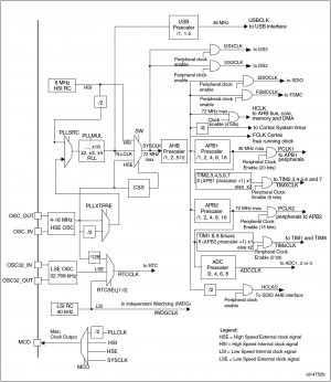
Clocks
HSI (8 MHz internal RC oscillator)
HSE (8 MHz external crystal oscillator)
LSI (40 kHz internal RC - watchdog, RTCCLK)
LSE (32768 Hz external crystal (RTCCLK))

PLLCLK  - Output from PLL, 8-64 MHz in 4 MHz steps, 72-128 MHz in 8 MHz steps
SYSCLK  - PLLCLK, HSI or HSE
AHBCLK  - SYSCLK / AHB prescaler (this clock has no name in the datasheet, except AHB peripheral clock)
PCLK1   - AHBCLK / APB1 prescaler - APB1 bus (max 36 MHz)
PCLK2   - AHBCLK / APB2 prescaler - APB2 bus (max 72 MHz)
USBCLK  - PLLCLK / USB prescaler
I2SCLK  - SYSCLK
SDIOCLK - AHBCLK
FSMCCLK - AHBCLK
FCLK    - AHBCLK
ADCCLK  - AHBCLK / (APB2 prescaler * ADC prescaler)

The MCO pin (PA8) can output one of SYSCLK, HSI, HSE, PLLCLK / 2
When the HSI is the PLL clock input, maximum system clock frequency is 64 MHz.
The SDIO AHB interface is clocked with a fixed frequency equal to AHBCLK / 2.
If the APB prescaler is 1, timers run at PCLK else at 2 * PCLK
Flash memory
- 0-24 MHz - zero wait state
- 24-48 MHz - one wait state
- 48-72 MHz - two wait states
The prefetch buffer must be switched on/off only when SYSCLOCK is lower than 24 MHz.
Pins with special functions
PA9  ----------> ICL3232
PA10 <--|100R|-- ICL3232
PB2  - Boot1 22 kOhm to +3.3 V or Gnd
PC14 - 32 kHz crystal
PC15 - 32 kHz crystal
PD0  - 8 MHz crystal
PD1  - 8 MHz crystal

The JTAG pins are in input PU/PD after reset:
 PA15: JTDI in PU
 PA14: JTCK in PD
 PA13: JTMS in PU
 PB4: NJTRST in PU
Peripherials
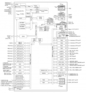
64 kB SRAM, 512 kB FLASH
3 x 12 bit A/D converters
2 x 12 bit D/A converters
5 x USART
2 x Advanced-control timers (TIM1 and TIM8) can each be seen as a three-phase PWM multiplexed on 6 channels.
4 x General purpose timer TIM2, TIM3, TIM4 and TIM5 - 16-bit auto-reload up/down counter, a 16-bit prescaler and feature 4 independent channels each for input capture/output compare, PWM or onepulse mode output. This gives up to 16 input captures / output compares / PWMs
2 x Basic timer TIM6 and TIM7 - These timers are mainly used for DAC trigger generation. They can also be used as a generic 16-bit time base.
3 x SPI
2 x I2S (multiplexed on SPI pins)
2 × I2C
1 x SD card interface 1/4/8 bit
1 x USB full speed
1 x CAN network interface
1 x CRC (cyclic redundancy check) calculation unit
1 x 24 bit systick timer
1 x RTC (real-time clock) and backup registers
2 x DMA controller, 5 + 7 channels
1 x Temperature sensor
A/D converters
- ADC1_IN17 is connected to VREFINT 1.2 V (1.16 V - 1.24 V)
- ADC1_IN16 is connected to the Temperature sensor
- ADC2_IN16 and ADC2_IN17 are connected to VSS
- ADC3_IN9, ADC3_IN14, ADC3_IN15, ADC3_IN16 and ADC3_IN17 are connected to VSS
The recommended sampling time for the internal channels is 17.1 μs. The TSVREFE bit must be set to enable both internal channels.
Flash uploader
Command line parameters for STMFlashLoader.exe:
-c --pn 3 --br 115200 --db 8 --sb 1 --to 1000 -i "STM32_High-density_512K" -e --all -d --fn "#H" --v
--pn 3 indicates com port: COM3
Important things to remember
- Registers need a clock to latch the data, so enable all the the upstream clocks before trying to configure a peripheral
- Pins with special functions
Pinout
Pin    Function1   Function2   Function3  Function4
-------------------------------------------------------
 PA0 - WKUP        USART2_CTS  ADC0       TIM2_CH1_ETR
 PA1 - USART2_RTS  ADC1        TIM2_CH2
 PA2 - USART2_TX   ADC2        TIM2_CH3
 PA3 - USART2_RX   ADC3        TIM2_CH4
 PA4 - SPI1_NSS    USART2_CK   ADC4
 PA5 - SPI1_SCK    ADC5
 PA6 - SPI1_MISO   ADC6        TIM3_CH1
 PA7 - SPI1_MOSI   ADC7        TIM3_CH2
 PA8 - USART1_CK   TIM1_CH1    MCO
 PA9 - USART1_TX   TIM1_CH2
PA10 - USART1_RX   TIM1_CH3
PA11 - USART1_CTS  CANRX       TIM1_CH4   USBDM
PA12 - USART1_RTS  CANTX       TIM1_ETR   USBDP
PA13 - JTMS        SWDIO
PA14 - JTCK        SWCLK
PA15 - JTDI        TIM2_CH1    SPI1_NSS

 PB0 - ADC8        TIM3_CH3
 PB1 - ADC9        TIM3_CH4
 PB2 - BOOT1
 PB3 - JTDO        TIM2_CH2    SPI1_SCK
 PB4 - JNTRST      TIM3_CH1    SPI1_MISO
 PB5 - I2C1_SMBAI  TIM3_CH2    SPI1_MOSI
 PB6 - I2C1_SCL    TIM4_CH1    USART1_TX
 PB7 - I2C1_SDA    TIM4_CH2    USART1_RX
 PB8 - TIM4_CH3    I2C1_SCL    CANRX
 PB9 - TIM4_CH4    I2C1_SDA    CANTX
PB10 - I2C2_SCL    USART3_TX   TIM2_CH3
PB11 - I2C2_SDA    USART3_RX   TIM2_CH4
PB12 - SPI2_NSS    I2C2_SMBAI  USART3_CK  TIM1_BKIN
PB13 - SPI2_SCK    USART3_CTS  TIM1_CH1N
PB14 - SPI2_MISO   USART3_RTS  TIM1_CH2N
PB15 - SPI2_MOSI   TIM1_CH3N

 PC0 - ADC10
 PC1 - ADC11
 PC2 - ADC12
 PC3 - ADC13
 PC4 - ADC14
 PC5 - ADC15
 PC6 - TIM3_CH1
 PC7 - TIM3_CH2
 PC8 - TIM3_CH3
 PC9 - TIM3_CH4
PC10 - USART3_TX
PC11 - USART3_RX
PC12 - USART3_CK
PC13 - TAMPER-RTC
PC14 - OSC32_IN
PC15 - OSC32_OUT

 PD0 - OSC_IN
 PD1 - OSC_OUT
 PD2 - TIM3_ETR

