- 256 MB DDR3L memory and 16 MB Quad-SPI Flash
- Programmable from JTAG and Quad-SPI flash
- 100 MHz & 12MHz external clocks
- Internal ADC Dual-channel, 1 MSPS
- Powered from USB or any 7V-15V source
- Interaction and Sensory Devices
- 4 Switches
- 4 Buttons
- 1 Board Reset Button
- 1 FPGA Reset Button
- 4 Green LEDs
- 2 RGB LEDs
- Expansion Connectors:
|
|
XC7S50-1CSGA324C
|
XC7S25-1CSGA324
|
| Logic Slices
|
8150
|
3650
|
| 6-Input LUTs
|
32 600
|
14 600
|
| Flip-Flops
|
65 200
|
29 200
|
| Block RAM
|
75 * 4500 = 337.5 KByte
|
45 * 4500 = 202.5 KByte
|
| DSP Slices
|
120
|
80
|
| Clock resources
|
5 PLLs
|
3 PLLs
|
Pmod interface
| Pinout of Pmod connector
|
| 3V3
|
GND
|
d3
|
d2
|
d1
|
d0
|
| 3V3
|
GND
|
d3
|
d2
|
d1
|
d0
|
- The 6 pin interface is one horizontal row on the connector.
- The 12 pin interface use both rows, a module can use several connectors.
- Port JA and JB are unprotected and routed for high speed.
- Port JC and JD are protected with 200 Ohm series resistors and are shared with the Arduino shield interface (IO34-IO41 IO26-IO33)
|
|
Pmod JA
|
Pmod JB
|
Pmod JC
|
Pmod JD
|
| Pmod Type
|
High-Speed
|
High-Speed
|
Standard
|
Standard
|
| Series resistor
|
0 Ohm
|
0 Ohm
|
200 Ohm
|
200 Ohm
|
| Shared pins
|
–
|
–
|
IO34-IO41
|
IO26-IO33
|
| Pin 1
|
L17
|
P17
|
U15
|
V15
|
| Pin 2
|
L18
|
P18
|
V16
|
U12
|
| Pin 3
|
M14
|
R18
|
U17
|
V13
|
| Pin 4
|
N14
|
T18
|
U18
|
T12
|
| Pin 7
|
M16
|
P14
|
U16
|
T13
|
| Pin 8
|
M17
|
P15
|
P13
|
R11
|
| Pin 9
|
M18
|
N15
|
R13
|
T11
|
| Pin 10
|
N18
|
P16
|
V14
|
U11
|
Arduino shield/chipKIT interface
45 total FPGA I/O (16 shared with Pmod connectors - IO34-IO41 IO26-IO33)
6 Single-ended 0-3.3V Analog inputs to XADC
3 (4 *S7-25) Differential 0-1.0V Analog input pairs to XADC
USB-UART bridge
- FTDI FT2232HQ USB-UART bridge with both JTAG and RS-232 ports
- JTAG is connected to the JTAG port on the FPGA
- RS-232 is connected to pin V12 and R12
- Two on-board status LEDs: the transmit LED (LD8) and the receive LED (LD7) (relative to the PC).
- Speed up to 12 MBit/s
Block RAM
Each block RAM stores up to 36 Kbits of dual ported RAM and has a FIFO controller and a ECC unit.
Each 36 Kbit block can be configured as two independent 18 Kb dual ported RAM.
Two adjacent 36 Kbit blocks can be configured as a 64Kb x 1 RAM.
Each 36 Kbit block RAM can be configured as a 32K x 1, 16K x 2, 8K x 4, 4K x 9, 2K x 18, 1K x 36, or 512 x 72 in simple dual-port mode.
Each 18 Kbit block RAM can be configured as a 16K x 1, 8K x2 , 4K x 4, 2K x 9, 1K x 18 or 512 x 36 in simple dual-port mode.
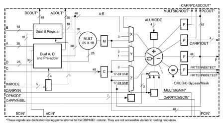
DSP48E1 slice
- 25-bit pre-adder with D register to enhance the capabilities of the A path
- INMODE control supports balanced pipelining when dynamically switching between multiply (A*B) and add operations (A:B)
- 25 x 18 multiplier
- 30-bit A input of which the lower 25 bits feed the A input of the multiplier, and the entire 30-bit input forms the upper 30 bits of the 48-bit A:B concatenate internal bus.
- Cascading A and B input
- Semi-independently selectable pipelining between direct and cascade paths
- Separate clock enables two-deep A and B set of input registers
- Independent C input and C register with independent reset and clock enable.
- CARRYCASCIN and CARRYCASCOUT internal cascade signals to support 96-bit accumulators/adders/subtracters in two DSP48E1 slices
- MULTSIGNIN and MULTSIGNOUT internal cascade signals with special OPMODE setting to support a 96-bit MACC extension
- Single Instruction Multiple Data (SIMD) Mode for three-input adder/subtracter which precludes use of multiplier in first stage
- Dual 24-bit SIMD adder/subtracter/accumulator with two separate CARRYOUT signals
- Quad 12-bit SIMD adder/subtracter/accumulator with four separate CARRYOUT signals
- 48-bit logic unit
- Bitwise logic operations – two-input AND, OR, NOT, NAND, NOR, XOR, and XNOR
- Logic unit mode dynamically selectable via ALUMODE
- Pattern detector
- Overflow/underflow support
- Convergent rounding support
- Terminal count detection support and auto resetting
- Cascading 48-bit P bus supports internal low-power adder cascade
- The 48-bit P bus allows for 12-bit/QUAD or 24-bit/DUAL SIMD adder cascade support
- Optional 17-bit right shift to enable wider multiplier implementation
- Dynamic user-controlled operating modes
- 7-bit OPMODE control bus provides X, Y, and Z multiplexer select signals
- Carry in for the second stage adder
- Support for rounding
- Support for wider add/subtracts
- 3-bit CARRYINSEL multiplexer
- Carry out for the second stage adder
- Support for wider add/subtracts
- Available for each SIMD adder (up to four)
- Cascaded CARRYCASCOUT and MULTSIGNOUT allows for MACC extensions up to 96 bits
- Optional input, pipeline, and output/accumulate registers
- Optional control registers for control signals (OPMODE, ALUMODE, and CARRYINSEL)
- Independent clock enable and resets for greater flexibility, with reset having priority.
- To save power when the first stage multiplier is not being used, the USE_MULT attribute allows the customer to gate off internal multiplier logic.
Files and information
