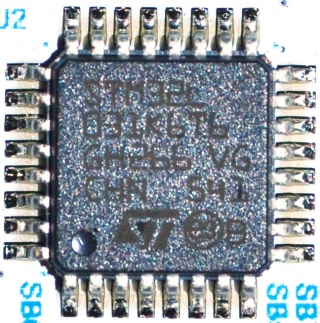
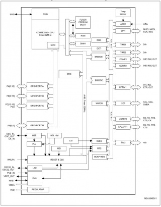
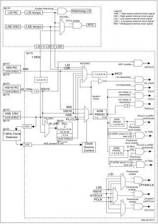
STM32L031K6 Microcontroller
From ScienceZero
Contents
STM32L031K6 Microcontroller Overview
- Ultra-low-power platform
- 1.65 V to 3.6 V power supply
- -40 to 125 °C temperature range
- 0.25 μA Standby mode (2 wakeup pins)
- 0.38 μA Stop mode (16 wakeup lines)
- 0.68 μA Stop mode + RTC + 8 KB RAM retention
- Down to 76 μA/MHz in Run mode
- 5 μs wakeup time (from Flash memory)
- 41 μA 12-bit ADC conversion (at 10ksps)
- Core: ARM® 32-bit Cortex®-M0+
- From 32 kHz up to 32 MHz max.
- 0.95 DMIPS/MHz
- Ultra-safe, low-power BOR (brownout reset) with 5 selectable thresholds
- Ultralow power POR/PDR
- Programmable voltage detector (PVD)
- Clock sources
- 1 to 25 MHz crystal oscillator
- 32 kHz oscillator for RTC with calibration
- High speed internal 16 MHz factory-trimmed RC (+/- 1%)
- Internal low-power 37 kHz RC
- Internal multispeed low-power 65 kHz to 4.2 MHz RC
- PLL for CPU clock
- Pre-programmed bootloader
- USART, SPI supported
- Development support
- Serial wire debug supported
- Up to 38 fast I/Os (31 I/Os 5V tolerant)
- Memories
- Up to 32 KB Flash with ECC
- 8 KB RAM
- 1 KB of data EEPROM with ECC
- 20-byte backup register
- Sector protection against R/W operation
- Rich Analog peripherals
- 12-bit ADC 1.14 Msps up to 10 channels (down to 1.65 V)
- 2x ultra-low-power comparators (window mode and wake up capability, down to 1.8 V)
- 7-channel DMA controller, supporting ADC, SPI, I2C, USART, Timers
- 5x peripherals communication interface
- 1x USART (ISO 7816, IrDA), 1x UART (low power)
- 1x SPI 16 Mbits/s
- 1x I2C (SMBus/PMBus)
- 8x timers: 1x 16-bit with up to 4 channels, 2x 16-bit with up to 2 channels, 1x 16-bit ultra-low-power timer, 1x SysTick, 1x RTC and 2x watchdogs (independent/window)
- CRC calculation unit, 96-bit unique ID
- All packages are ECOPACK®2
Documents and files
Datasheet
Specifications
Getting started
Reference manual
Programming manual
Errata
Getting started with STM32F0 or STM32L0 series
Virtually increasing the number of serial communication peripherals in STM32 applications
Guidelines to increase the number of touch sensing touchkeys
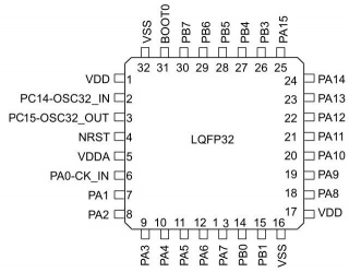
Pinout
Alternate function mapping
| Pin | AF0 | AF1 | AF2 | AF3 | AF4 | AF5 | AF6 | AF7 | Additional functions |
|---|---|---|---|---|---|---|---|---|---|
| PA0 | USART1_CTS | TIM2_CH1_ETR |
ADC_IN0 | ||||||
| PA1 | EVENTOUT | USART1_RTS | TIM2_CH2 | ADC_IN1 | |||||
| PA2 | USART1_TX | TIM2_CH3 | ADC_IN2 | ||||||
| PA3 | USART1_RX | TIM2_CH4 | ADC_IN3 | ||||||
| PA4 |
SPI1_NSS |
USART1_CK | TIM14_CH1 | ADC_IN4 | |||||
| PA5 |
SPI1_SCK |
TIM2_CH1_ETR | ADC_IN5 | ||||||
| PA6 |
SPI1_MISO |
TIM3_CH1 | TIM1_BKIN | TIM16_CH1 | EVENTOUT | ADC_IN6 | |||
| PA7 |
SPI1_MOSI |
TIM3_CH2 | TIM1_CH1N | TIM14_CH1 | TIM17_CH1 | EVENTOUT | ADC_IN7 | ||
| PA8 | MCO | USART1_CK | TIM1_CH1 | EVENTOUT | |||||
| PA9 | USART1_TX | TIM1_CH2 | I2C1_SCL | ||||||
| PA10 | TIM17_BKIN | USART1_RX | TIM1_CH3 | I2C1_SDA | |||||
| PA11 | EVENTOUT | USART1_CTS | TIM1_CH4 | ||||||
| PA12 | EVENTOUT | USART1_RTS | TIM1_ETR | ||||||
| PA13 | SWDIO | IR_OUT | |||||||
| PA14 | SWCLK | USART1_TX | |||||||
| PA15 |
SPI1_NSS |
USART1_RX | TIM2_CH1_ETR | EVENTOUT | |||||
| PB0 | EVENTOUT | TIM3_CH3 | TIM1_CH2N | ADC_IN8 | |||||
| PB1 | TIM14_CH1 | TIM3_CH4 | TIM1_CH3N | ADC_IN9 | |||||
| PB2 | |||||||||
| PB3 | SPI1_SCK
I2S1_CK |
EVENTOUT | TIM2_CH2 | ||||||
| PB4 |
SPI1_MISO |
TIM3_CH1 | EVENTOUT | ||||||
| PB5 |
SPI1_MOSI |
TIM3_CH2 | TIM16_BKIN | I2C1_SMBA | |||||
| PB6 | USART1_TX | I2C1_SCL | TIM16_CH1N | ||||||
| PB7 | USART1_RX | I2C1_SDA | TIM17_CH1N | ||||||
| PF0 | OSC_IN | ||||||||
| PF1 | OSC_OUT |
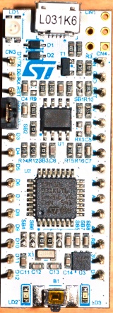
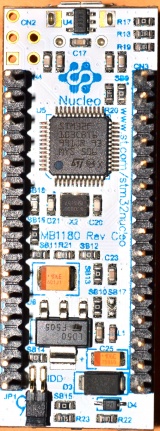
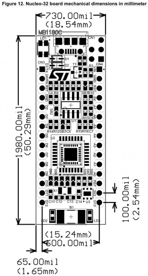
NUCLEO-L031K6 development Board Overview
| Front | Back | Dimentions |
|---|---|---|
|
|
|
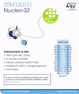
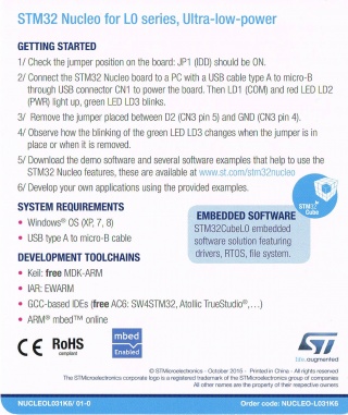
Packaging literature
| Front | Back |
|---|---|
|
|
Features
- STM32 microcontrollers in 32-pin packages
- Extension with Arduino™ nano connectivity
- ARM® mbed™ -enabled (see http://mbed.org)
- On-board ST-LINK/V2-1 debugger/programmer with SWD connector:
- USB VBUS
- External source
- Three LEDs:
- USB communication (LD1), power LED (LD2), user LED (LD3)
- Reset push-button
- Supported by wide choice of Integrated Development Environments (IDEs) including IAR™ , Keil® , GCC-based IDEs (AC6 SW4STM32, ...)
Documents and files
Specifications
Getting started with STM32 Nucleo board software development tools
User manual
Schematic
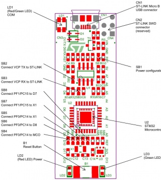
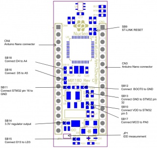
Board Layout
| Top | Bottom |
|---|---|
|
|
Pinout
Available pins on board
| Bit | 0 | 1 | 2 | 3 | 4 | 5 | 6 | 7 | 8 | 9 | 10 | 11 | 12 | 13 | 14 | 15 |
| Port A | PA0 | PA1 | PA2 | PA3 | PA4 | PA5 | PA6 | PA7 | PA8 | PA9 | PA10 | PA11 | PA12 | |||
| Port B | PB0 | PB1 | PB3 | PB4 | PB5 | PB6 | PB7 | |||||||||
| Port F | PF0 | PF1 |
PCB IO map
| STM32 pin | Board pin name | Board pin number | Direction | Connected to | Alternate functions | Notes |
| PA0 | A0 | CN4.12 | ↔ |
|
|
|
| PA1 | A1 | CN4.11 | ↔ |
|
|
|
| PA2 | A7 | CN4.5 | → |
|
|
|
| PA3 | A2 | CN4.10 | ↔ |
|
|
|
| PA4 | A3 | CN4.9 | ↔ |
|
|
|
| PA5 | A4 | CN4.8 | ↔ |
|
|
Limitations on A4 and A5, D4 and D5 related to I2C configuration are explained in Section 6.8: Solder bridges according to SB16/SB18 setting. |
| PA6 | A5 | CN4.7 | ↔ |
|
|
Limitations on A4 and A5, D4 and D5 related to I2C configuration are explained in Section 6.8: Solder bridges according to SB16/SB18 setting. |
| PA7 | A6 | CN4.6 | ↔ |
|
|
|
| PA8 | D9 | CN3.12 | ↔ |
|
|
|
| PA9 | D1 | CN3.1 | → |
|
|
Only one USART is available and it is shared between Arduino Nano and VCP. The selection is done by remapping (no need to change the hardware configuration). |
| PA10 | D0 | CN3.2 | ← |
|
|
Only one USART is available and it is shared between Arduino Nano and VCP. The selection is done by remapping (no need to change the hardware configuration). |
| PA11 | D10 | CN3.13 | ↔ |
|
|
SPI_CS is made by GPIO. |
| PA12 | D2 | CN3.5 | ↔ |
|
||
| PB0 | D3 | CN3.6 | ↔ |
|
|
|
| PB1 | D6 | CN3.9 | ↔ |
|
|
|
| PB3 | D13 | CN4.15 | ↔ |
|
|
|
| PB4 | D12 | CN3.15 | ↔ |
|
|
|
| PB5 | D11 | CN3.14 | ↔ |
|
|
|
| PB6 | D5 | CN3.8 | ↔ |
|
|
D5 PWM on inverted channel Timer 16. |
| PB7 | D4 | CN3.7 | ↔ |
|
||
| PF0 | D7 | CN3.10 | ↔ |
|
D7/D8 shared with OSC_IN/OSC_OUT. | |
| PF1 | D8 | CN3.11 | ↔ |
|
D7/D8 shared with OSC_IN/OSC_OUT. |
