STM32L031K6 Microcontroller
From ScienceZero
Revision as of 12:35, 14 June 2016 by Avi (Talk | contribs) (→NUCLEO-F031K6 development Board Overview)
Contents
STM32F031K6 Microcontroller Overview
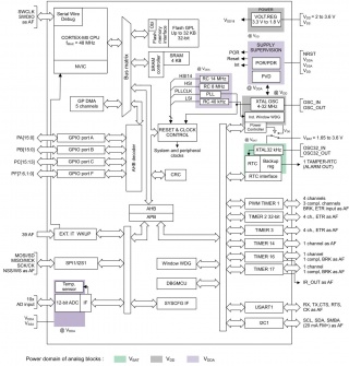
- Core: ARM® 32-bit Cortex® -M0 CPU, frequency up to 48 MHz
- Memories
- 16 to 32 Kbytes of Flash memory
- 4 Kbytes of SRAM with HW parity
- CRC calculation unit
- Reset and power management
- Digital and I/Os supply: 2.0 to 3.6 V
- Analog supply: VDDA = from VDD to 3.6 V
- Power-on/Power-down reset (POR/PDR)
- Programmable voltage detector (PVD)
- Low power modes: Sleep, Stop and Standby
- VBAT supply for RTC and backup registers
- Clock management
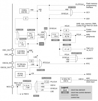
- 4 to 32 MHz crystal oscillator
- 32 kHz oscillator for RTC with calibration
- Internal 8 MHz RC with x6 PLL option
- Internal 40 kHz RC oscillator
- Up to 39 fast I/Os
- All mappable on external interrupt vectors
- Up to 26 I/Os with 5 V tolerant capability
- 5-channel DMA controller
- 1 × 12-bit, 1.0 μs ADC (up to 10 channels)
- Conversion range: 0 to 3.6V
- Separate analog supply from 2.4 up to 3.6 V
- Up to 9 timers
- 1 x 16-bit 7-channel advanced-control timer for 6 channels PWM output, with deadtime generation and emergency stop
- 1 x 32-bit and 1 x 16-bit timer, with up to 4 IC/OC, usable for IR control decoding
- 1 x 16-bit timer, with 2 IC/OC, 1 OCN, deadtime generation and emergency stop
- 1 x 16-bit timer, with IC/OC and OCN, deadtime generation, emergency stop and modulator gate for IR control
- 1 x 16-bit timer with 1 IC/OC
- Independent and system watchdog timers
- SysTick timer: 24-bit downcounter
- Calendar RTC with alarm and periodic wakeup from Stop/Standby
- Communication interfaces
- 1 x I2 C interface, supporting Fast Mode Plus (1 Mbit/s) with 20 mA current sink, SMBus/PMBus, and wakeup from Stop mode
- 1 x USART supporting master synchronous SPI and modem control, ISO7816 interface, LIN, IrDA capability auto baud rate detection and wakeup feature
- 1 x SPI (18 Mbit/s) with 4 to 16 programmable bit frames, with I2 S interface multiplexed
- Serial wire debug (SWD)
- 96-bit unique ID
- Extended temperature range: -40 to +105°C
- All packages ECOPACK® 2
Memory map
*I = Instruction bus, D = Data bus, S = System bus
Documents and files
Datasheet
Specifications
Getting started
Reference manual
Programming manual
Getting started with STM32F0
STM32 - 32-bit ARM Cortex-M MCUs
Migrating between STM32F1 and STM32F0 series microcontrollers
Errata
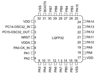
Pinout
Alternate function mapping
| Pin | AF0 | AF1 | AF2 | AF3 | AF4 | AF5 | AF6 | AF7 | Additional functions |
|---|---|---|---|---|---|---|---|---|---|
| PA0 | USART1_CTS | TIM2_CH1_ETR |
ADC_IN0 | ||||||
| PA1 | EVENTOUT | USART1_RTS | TIM2_CH2 | ADC_IN1 | |||||
| PA2 | USART1_TX | TIM2_CH3 | ADC_IN2 | ||||||
| PA3 | USART1_RX | TIM2_CH4 | ADC_IN3 | ||||||
| PA4 |
SPI1_NSS |
USART1_CK | TIM14_CH1 | ADC_IN4 | |||||
| PA5 |
SPI1_SCK |
TIM2_CH1_ETR | ADC_IN5 | ||||||
| PA6 |
SPI1_MISO |
TIM3_CH1 | TIM1_BKIN | TIM16_CH1 | EVENTOUT | ADC_IN6 | |||
| PA7 |
SPI1_MOSI |
TIM3_CH2 | TIM1_CH1N | TIM14_CH1 | TIM17_CH1 | EVENTOUT | ADC_IN7 | ||
| PA8 | MCO | USART1_CK | TIM1_CH1 | EVENTOUT | |||||
| PA9 | USART1_TX | TIM1_CH2 | I2C1_SCL | ||||||
| PA10 | TIM17_BKIN | USART1_RX | TIM1_CH3 | I2C1_SDA | |||||
| PA11 | EVENTOUT | USART1_CTS | TIM1_CH4 | ||||||
| PA12 | EVENTOUT | USART1_RTS | TIM1_ETR | ||||||
| PA13 | SWDIO | IR_OUT | |||||||
| PA14 | SWCLK | USART1_TX | |||||||
| PA15 |
SPI1_NSS |
USART1_RX | TIM2_CH1_ETR | EVENTOUT | |||||
| PB0 | EVENTOUT | TIM3_CH3 | TIM1_CH2N | ADC_IN8 | |||||
| PB1 | TIM14_CH1 | TIM3_CH4 | TIM1_CH3N | ADC_IN9 | |||||
| PB2 | |||||||||
| PB3 | SPI1_SCK
I2S1_CK |
EVENTOUT | TIM2_CH2 | ||||||
| PB4 |
SPI1_MISO |
TIM3_CH1 | EVENTOUT | ||||||
| PB5 |
SPI1_MOSI |
TIM3_CH2 | TIM16_BKIN | I2C1_SMBA | |||||
| PB6 | USART1_TX | I2C1_SCL | TIM16_CH1N | ||||||
| PB7 | USART1_RX | I2C1_SDA | TIM17_CH1N | ||||||
| PF0 | OSC_IN | ||||||||
| PF1 | OSC_OUT |
NUCLEO-L031K6 development Board Overview
| Front | Back | Dimentions |
|---|---|---|
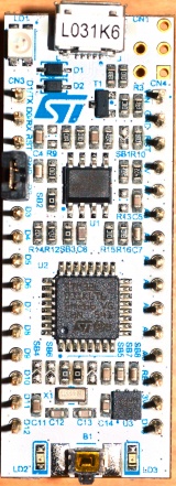
|
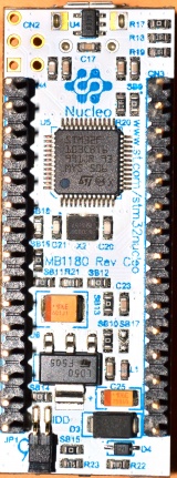
|
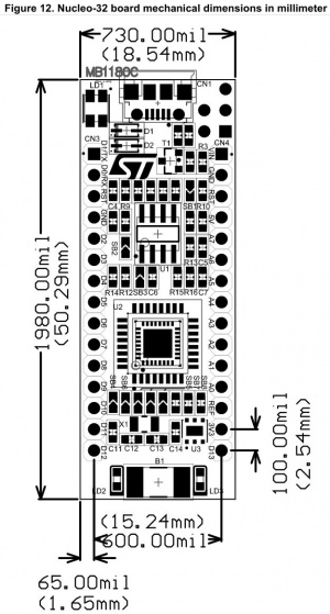
|
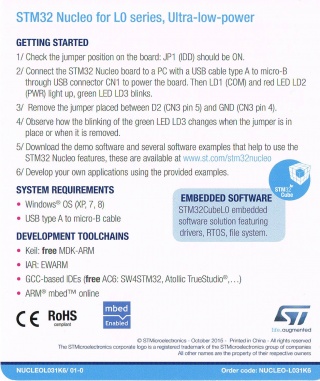
Packaging literature
| Front | Back |
|---|---|
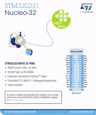
|
|
Features
- STM32 microcontrollers in 32-pin packages
- extension with Arduino™ nano connectivity
- mbed-enabled (http://mbed.org)
- on-board ST-LINK/V2-1 debugger/programmer
- USB reenumeration capability: three different interfaces supported on USB:
- Virtual Com port
- mass storage
- debug port
- flexible board power supply:
- USB VBUS
- external source
- three LEDs:
- USB communication (LD1)
- power LED (LD2)
- user LED (LD3)
- reset push button
- supported by wide choice of Integrated Development Environments (IDEs) including IAR™, Keil®, GCC-based IDEs (AC6 SW4STM32, ...)
Documents and files
STM32 Nucleo-32 board specifications
Getting started with STM32 Nucleo board software development tools
User manual
Shematic
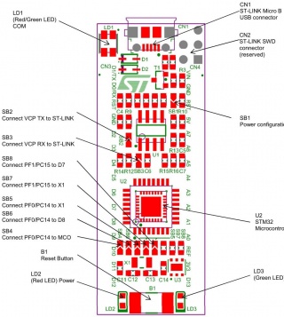
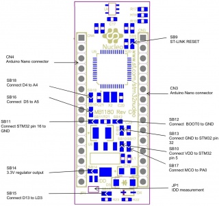
Board Layout
| Top | Bottom |
|---|---|
|
|
Pinout
Available pins on board
| Bit | 0 | 1 | 2 | 3 | 4 | 5 | 6 | 7 | 8 | 9 | 10 | 11 | 12 | 13 | 14 | 15 |
| Port A | PA0 | PA1 | PA2 | PA3 | PA4 | PA5 | PA6 | PA7 | PA8 | PA9 | PA10 | PA11 | PA12 | |||
| Port B | PB0 | PB1 | PB3 | PB4 | PB5 | PB6 | PB7 | |||||||||
| Port F | PF0 | PF1 |
PCB IO map
| STM32 pin | Board pin name | Board pin number | Direction | Connected to | Alternate functions | Notes |
| PA0 | A0 | CN4.12 | ↔ |
|
|
|
| PA1 | A1 | CN4.11 | ↔ |
|
|
|
| PA2 | A7 | CN4.5 | → |
|
|
|
| PA3 | A2 | CN4.10 | ↔ |
|
|
|
| PA4 | A3 | CN4.9 | ↔ |
|
|
|
| PA5 | A4 | CN4.8 | ↔ |
|
|
Limitations on A4 and A5, D4 and D5 related to I2C configuration are explained in Section 6.8: Solder bridges according to SB16/SB18 setting. |
| PA6 | A5 | CN4.7 | ↔ |
|
|
Limitations on A4 and A5, D4 and D5 related to I2C configuration are explained in Section 6.8: Solder bridges according to SB16/SB18 setting. |
| PA7 | A6 | CN4.6 | ↔ |
|
|
|
| PA8 | D9 | CN3.12 | ↔ |
|
|
|
| PA9 | D1 | CN3.1 | → |
|
|
Only one USART is available and it is shared between Arduino Nano and VCP. The selection is done by remapping (no need to change the hardware configuration). |
| PA10 | D0 | CN3.2 | ← |
|
|
Only one USART is available and it is shared between Arduino Nano and VCP. The selection is done by remapping (no need to change the hardware configuration). |
| PA11 | D10 | CN3.13 | ↔ |
|
|
SPI_CS is made by GPIO. |
| PA12 | D2 | CN3.5 | ↔ |
|
||
| PB0 | D3 | CN3.6 | ↔ |
|
|
|
| PB1 | D6 | CN3.9 | ↔ |
|
|
|
| PB3 | D13 | CN4.15 | ↔ |
|
|
|
| PB4 | D12 | CN3.15 | ↔ |
|
|
|
| PB5 | D11 | CN3.14 | ↔ |
|
|
|
| PB6 | D5 | CN3.8 | ↔ |
|
|
D5 PWM on inverted channel Timer 16. |
| PB7 | D4 | CN3.7 | ↔ |
|
||
| PF0 | D7 | CN3.10 | ↔ |
|
D7/D8 shared with OSC_IN/OSC_OUT. | |
| PF1 | D8 | CN3.11 | ↔ |
|
D7/D8 shared with OSC_IN/OSC_OUT. |
