STM32F429 Microcontroller
From ScienceZero
Revision as of 06:34, 31 January 2014 by Avi (Talk | contribs) (→32F429IDISCOVERY Development Board Overview)
Contents
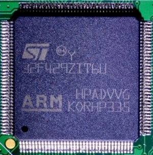
STM32F429ZIT6 Microcontroller Overview
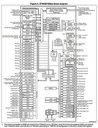
- ARM Cortex-M4 32b MCU+FPU, 225DMIPS, up to 2MB Flash/256+4KB RAM, USB OTG HS/FS, Ethernet, 17 TIMs, 3 ADCs, 20 comm. interfaces, camera & LCD-TFT, Adaptive real-time accelerator (ART AcceleratorTM) allowing 0-wait state execution from Flash memory, frequency up to 180 MHz, and DSP instructions
- Memories
- Up to 2 MB of Flash memory organized into two banks allowing read-while-write
- Up to 256+4 KB of SRAM including 64-KB of CCM (core coupled memory) data RAM
- Flexible external memory controller with up to 32-bit data bus: SRAM,PSRAM,SDRAM, Compact Flash/NOR/NAND memories
- LCD parallel interface, 8080/6800 modes
- LCD-TFT controller up to VGA resolution with dedicated Chrom-ART AcceleratorTM for enhanced graphic content creation (DMA2D)
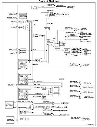
- Clock, reset and supply management
- 1.8 V to 3.6 V application supply and I/Os
- POR, PDR, PVD and BOR
- 4-to-26 MHz crystal oscillator
- Internal 16 MHz factory-trimmed RC (1% accuracy)
- 32 kHz oscillator for RTC with calibration
- Internal 32 kHz RC with calibration
- Low power
- Sleep, Stop and Standby modes
- VBAT supply for RTC, 20×32 bit backup registers + optional 4 KB backup SRAM
- 3×12-bit, 2.4 MSPS ADC: up to 24 channels and 7.2 MSPS in triple interleaved mode
- 2×12-bit D/A converters
- General-purpose DMA: 16-stream DMA controller with FIFOs and burst support
- Up to 17 timers: up to twelve 16-bit and two 32- bit timers up to 180 MHz, each with up to 4 IC/OC/PWM or pulse counter and quadrature (incremental) encoder input
- Debug mode
- SWD & JTAG interfaces
- Cortex-M4 Embedded Trace MacrocellTM
- Up to 168 I/O ports with interrupt capability
- Up to 164 fast I/Os upto 84MHz
- Up to 166 5 V-tolerant I/Os
- Up to 21 communication interfaces
- Up to 3 × I2C interfaces (SMBus/PMBus)
- Up to 4 USARTs/4 UARTs (11.25 Mbit/s, ISO7816 interface, LIN, IrDA, modem control)
- Up to 6 SPIs (42 Mbits/s), 2 with muxed full-duplex I2S for audio class accuracy via internal audio PLL or external clock
- 1 x SAI (serial audio interface)
- 2 × CAN (2.0B Active) and SDIO interface
- Advanced connectivity
- USB 2.0 full-speed device/host/OTG controller with on-chip PHY
- USB 2.0 high-speed/full-speed device/host/OTG controller with dedicated DMA, on-chip full-speed PHY and ULPI
- 10/100 Ethernet MAC with dedicated DMA: supports IEEE 1588v2 hardware, MII/RMII
- 8 to 14-bit parallel camera interface up to 54 MBs/s
- True random number generator
- CRC calculation unit
- 96-bit unique ID
- RTC: subsecond accuracy, hardware calendar
Documents and files
- Latest version of Keil µVision (Register for free to get the download link)
- STM32F429ZI microcontroller datasheet
- ARM Cortex®-M4 Technical Reference Manual
- STM32F42xxx Reference Manual
- Programming manual
- STM32F429ZI resources (click the Design Resources tab)
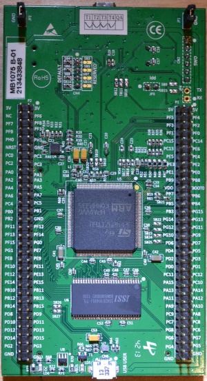
32F429IDISCOVERY Development Board Overview
- STM32F429ZIT6 microcontroller featuring
- 2 MB of Flash memory
- 256 KB of RAM
- LQFP144 package
- On-board ST-LINK/V2 with selection mode switch to use the kit as a standalone
- ST-LINK/V2 (with SWD connector for programming and debugging)
- Board power supply
- through the USB bus
- from an external 3 V or 5 V supply voltage
- 2.4" QVGA TFT LCD
- ILI9341 LCD controller
- SDRAM 64 Mbits
- L3GD20, ST MEMS motion sensor, 3-axis digital output gyroscope
- Six LEDs:
- LD1 (red/green) for USB communication
- LD2 (red) for 3.3 V power-on
- Two user LEDs
- LD3 (green) PG13
- LD4 (red) PG14
- Two USB OTG LEDs:
- LD5 (green) VBUS
- LD6 (red) OC (over-current)
- Two pushbuttons
- user
- reset
- USB OTG with micro-AB connector
- Extension header for LQFP144 I/Os for a quick connection to the prototyping board and an easy probing
Documents and files
- Product Page 32F429IDISCOVERYDiscovery kit for STM32 F429/439 lines - with STM32F429ZI MCU
- Discovery kit for STM32F429/439 lines board data brief
- Schematic
- User Manual Discovery kit for STM32F429/439 lines (board overview, diagrams and schematics, used pins)
- Getting started with the STM32F429 Discovery kit (connecting and programming)
- Getting started with STM32F429 Discovery software development tools (programming and IDEs)
- STSW-STM32138STM32F429 discovery firmware package (UM1662)
- STM32F429 discovery .Net Micro Framework package (UM1676)
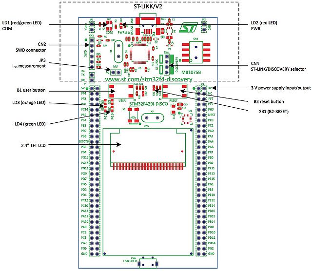
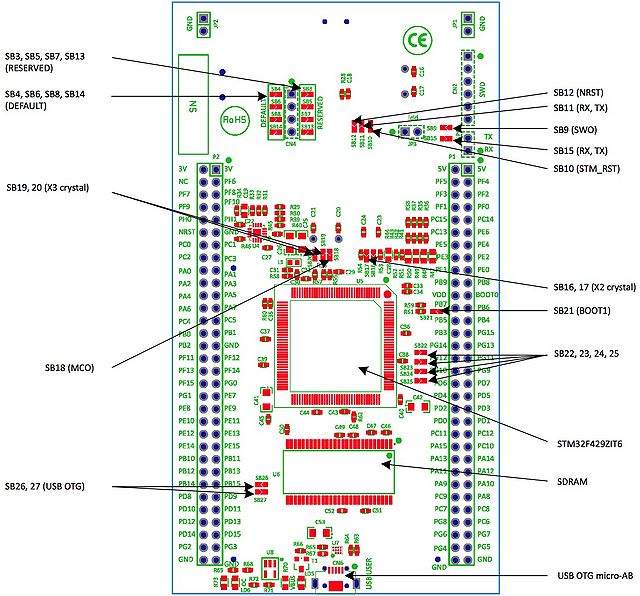
Board Layout
| Front View |
|
| Back View |
|
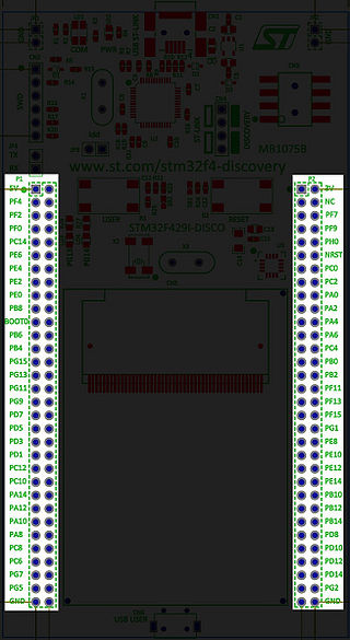
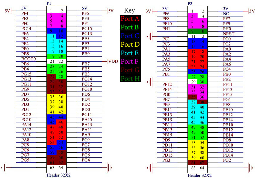
Pinout
Available pins on board
| Bit | 0 | 1 | 2 | 3 | 4 | 5 | 6 | 7 | 8 | 9 | 10 | 11 | 12 | 113 | 14 | 15 |
| Port A | PA0 | PA1 | PA2 | PA3 | PA4 | PA5 | PA6 | PA7 | PA8 | PA9 | PA10 | PA11 | PA12 | PA13 | PA14 | PA15 |
| Port B | PB3 | PB4 | PB5 | PB6 | PB7 | PB8 | PB9 | PB10 | PB11 | PB12 | PB13 | PB14 | PB15 | |||
| Port C | PC0 | PC1 | PC2 | PC3 | PC4 | PC5 | PC6 | PC7 | PC8 | PC9 | PC10 | PC11 | PC12 | PC13 | PC14 | PC15 |
| Port D | PD0 | PD1 | PD2 | PD3 | PD4 | PD5 | PD6 | PD7 | PD8 | PD9 | PD10 | PD11 | PD12 | PD13 | PD14 | PD15 |
| Port E | PE0 | PE1 | PE2 | PE3 | PE4 | PE5 | PE6 | PE7 | PE8 | PE9 | PE10 | PE11 | PE12 | PE13 | PE14 | PE15 |
| Port F | PF0 | PF1 | PF2 | PF3 | PF4 | PF5 | PF11 | PF12 | PF13 | PF14 | PF15 | |||||
| Port G | PG0 | PG1 | PG2 | PG3 | PG4 | PG5 | PG6 | PG7 | PG8 | PG9 | PG10 | PG11 | PG12 | PG13 | PG14 | PG15 |
| Port H | PH0 | PH1 |
PCB IO map
| Pin | Direction | Connected to |
| PA0 | ← |
|
| PA1 | ← |
|
| PA2 | ← |
|
| PA3 | ↔ |
|
| PA4 | ? |
|
| PA5 | ||
| PA6 | ↔ |
|
| PA7 | ? |
|
| PA8 | ? |
|
| PA9 | ||
| PA10 | ||
| PA11 | ↔ |
|
| PA12 | ↔ |
|
| PA13 | ? |
|
| PA14 | ? |
|
| PA15 | ← |
|
| PB0 | ↔ | |
| PB1 | ↔ | |
| PB2 | ↔ | |
| PB3 | ↔ | |
| PB4 | ↔ | |
| PB5 | ↔ | |
| PB6 | ↔ | |
| PB7 | ↔ | |
| PB8 | ↔ | |
| PB9 | ↔ | |
| PB10 | ↔ | |
| PB11 | ↔ | |
| PB12 | ↔ | |
| PB13 | ↔ | |
| PB14 | ↔ | |
| PB15 | ↔ | |
| PC0 | ↔ | |
| PC1 | ↔ | |
| PC2 | ↔ | |
| PC3 | ↔ | |
| PC4 | ↔ | |
| PC5 | ↔ | |
| PC6 | ↔ | |
| PC7 | ↔ | |
| PC8 | ↔ | |
| PC9 | ↔ | |
| PC10 | ↔ | |
| PC11 | ↔ | |
| PC12 | ↔ | |
| PC13 | ↔ | |
| PC14 | ↔ | |
| PC15 | ↔ | |
| PD0 | ↔ | |
| PD1 | ↔ | |
| PD2 | ↔ | |
| PD3 | ↔ | |
| PD4 | ↔ | |
| PD5 | ↔ | |
| PD6 | ↔ | |
| PD7 | ↔ | |
| PD8 | ↔ | |
| PD9 | ↔ | |
| PD10 | ↔ | |
| PD11 | ↔ | |
| PD12 | ↔ | |
| PD13 | ↔ | |
| PD14 | ↔ | |
| PD15 | ↔ | |
| PE0 | ↔ | |
| PE1 | ↔ | |
| PE2 | ↔ | |
| PE3 | ↔ | |
| PE4 | ↔ | |
| PE5 | ↔ | |
| PE6 | ↔ | |
| PE7 | ↔ | |
| PE8 | ↔ | |
| PE9 | ↔ | |
| PE10 | ↔ | |
| PE11 | ↔ | |
| PE12 | ↔ | |
| PE13 | ↔ | |
| PE14 | ↔ | |
| PE15 | ↔ | |
| PF0 | ↔ | |
| PF1 | ↔ | |
| PF2 | ↔ | |
| PF3 | ↔ | |
| PF4 | ↔ | |
| PF5 | ↔ | |
| PF6 | ↔ | |
| PF7 | ↔ | |
| PF8 | ↔ | |
| PF9 | ↔ | |
| PF10 | ↔ | |
| PF11 | ↔ | |
| PF12 | ↔ | |
| PF13 | ↔ | |
| PF14 | ↔ | |
| PF15 | ↔ | |
| PG0 | ↔ | |
| PG1 | ↔ | |
| PG2 | ↔ | |
| PG3 | ↔ | |
| PG4 | ↔ | |
| PG5 | ↔ | |
| PG6 | ↔ | |
| PG7 | ↔ | |
| PG8 | ↔ | |
| PG9 | ↔ | |
| PG10 | ↔ | |
| PG11 | ↔ | |
| PG12 | ↔ | |
| PG13 | ↔ | |
| PG14 | ↔ | |
| PG15 | ↔ | |
| PH0 | ↔ | |
| PH1 | ↔ | |
| PH2 | ↔ | |
| PH3 | ↔ | |
| PH4 | ↔ | |
| PH5 | ↔ | |
| PH6 | ↔ | |
| PH7 | ↔ | |
| PH8 | ↔ | |
| PH9 | ↔ | |
| PH10 | ↔ | |
| PH11 | ↔ | |
| PH12 | ↔ | |
| PH13 | ↔ | |
| PH14 | ↔ | |
| PH15 | ↔ |
